
No audio available for this content.
Fully Integrated NAPA Receiver Brings Mass-Market Potential
This integrated circuit supports simultaneous reception and processing of the GPS L1/L5, Galileo E1/E5a, and GLONASS G1 signals with 40 tracking channels. The dual-band analog RF front-end is integrated on the same mixed-signal chip as the baseband hardware, including an embedded processor to close the tracking loops: overall, a compact, low-power, and low-cost solution.
By Fabio Garzia, Stefan Köhler, Santiago Urquijo, Philipp Neumaier,Jörn Driesen, Sybille Haas, Thomas Leineweber, Tao Zhang, Sascha Krause, Frank Henkel,Alexander Rügamer, Matthias Overbeck, and Günther Rohmer
Multi-constellation multi-band global navigation satellite system (GNSS) receivers can efficiently exploit the advantages derived from the modernization of existing GNSS constellations, such as GPS and GLONASS, as well as from the launch of new ones like Galileo and BeiDou. Utilizing multiple systems can significantly improve the availability of a navigation solution in urban canyons and heavily shadowed areas. Increased satellite availability also guarantees higher measurement redundancy and improved reliability. Moreover, the excellent inherent noise and multipath mitigation capabilities of the new and modernized wideband signals in the L5/E5a band, combined with the ionosphere error mitigation given by frequency diversity, significantly improves the accuracy in both measurement and position domains.
Still, most commercial fully-integrated single-chip mass market GNSS receivers use only a single-frequency band for their positioning, velocity, time (PVT) solution: either GPS L1 C/A or Galileo E1 and GLONASS G1. For example, the Teseo chips are single-chip solutions that support multiple constellations but only on one frequency band. This approach reduces design costs and enables the lowest consumption of power, but neglects the advantages of wideband signal processing – which offers increased robustness thanks to two simultaneous frequency band receptions and the capability of mitigating the ionosphere error.
Another approach for realizing multi-constellation multi-frequency solutions is to combine different chips for the analog front-end and the digital baseband. One fully integrated single-chip analog multi-band front-end for the simultaneous reception of GPS L1/L5, Galileo E1/E5, and GLONASS has been presented. However, this chip included only the front-end and requires an additional, separate digital-baseband solution.
The purpose of the NAPA project (NAvigation chip for Pedestrian navigation and higher precision Applications) is to close this gap by providing a fully integrated, compact, low-power, and low-cost solution in which the analog and digital parts of the GNSS receiver are integrated together on the same chip. The NAPA receiver offers all the advantages of multi-constellation reception with additional dual-frequency support.
The NAPA chip features a monolithic, single mixed-signal chip implementation of a multi-system, multi-band analog front-end and the related digital baseband core, including an embedded processor. The NAPA chip can be used as a stand-alone GNSS sensor, because no additional components are required to obtain a PVT solution. The ASIC was implemented in a low-power technology and adopts some ad-hoc low-power architectural features. In regard to costs, an ASIC solution is more convenient than FPGA, provided the non-recurring engineering costs (NRE) are amortized by the amount of chips manufactured and sold. The NAPA chip supports multi-system (GPS, Galileo, and GLONASS) and multi-band (GPS/Galileo L1/E1, L5/E5a, GLONASS G1) processing. Figure 1 shows the frequency band being selected for receiving and processing in the NAPA chip. With two fully deployed GNSS — GPS and GLONASS — NAPA chips can already be used in many commercial applications. Thanks to the spectral overlay of the GPS L1/L5 and Galileo E1/E5a signals, the chip is also ready for Galileo. The frequency selection features both the narrow-band legacy signals L1/G1, which can be used for fast acquisition. For highest tracking accuracy, the wideband GPS L5 and Galileo E5a BPSK(10) modulated signals can be utilized.

The higher accuracy is obtained primarily by the attenuation of the ionospheric error. The ionosphere is a dispersing media that can introduce a bias error between 1 and 20 m. Forming a linear combination of two independent frequency-band measurements, the ionospheric bias can be measured and almost completely removed. In addition, Precise Point Positioning and Wide/Narrow-laning combinations are possible, thanks to the second received frequency band. The first allows for the combination of precise satellite positions and clocks with multi-frequency measurements, providing cm/dm solutions. The second adopts fast ambiguity solutions for carrier-phase positioning and cycle-slip detection.
In this article, we present the NAPA chip in detail. We describe the architecture of the analog front-end and its digital counterpart and the innovative features of each. Then we provide details about chip implementation, manufacturing, and test setup. Finally, we present the first verification results and draw conclusions.
Architecture Overview
The NAPA chip architecture, depicted in Figure 2, is composed of two separate blocks integrated on the same silicon die: the analog core provides the functionality of a two-frequency radio-frequency (RF) front-end, whereas the digital part implements the main GNSS processing tasks, including the correlator channels and an embedded processor, and takes care of the RF front-end control. The interface between the two blocks is completely digital and provides synchronizers to ensure a valid clock domain crossing (CDC).

Analog Front-End. The analog RF front-end supports the simultaneous reception of GPS L5 / Galileo E5a and GPS L1 / Galileo E1 / GLONASS G1 signals as well as modes where only one reception path is activated.
Both passive and active GNSS antennas are supported, thanks to integrated low noise amplifiers (LNA). There are two separate signal reception paths for the two frequency bands. The L1/E1/G1 path is characterized by a quasi-zero-IF conversion that mixes the middle frequency between L1/E1 and G1 to zero frequency. The L1/E1 reception bandwidth is up to 14 MHz so as to incorporate the MBOC modulations of Galileo E1 and future GPS L1C signals. A programmable automatic gain control (AGC) controls the complex analog baseband signals before they are digitized with a 4-bit dual-channel analog digital converter (ADC).
The second reception path receives an L5/E5a signal with up to 20 MHz bandwidth for the BPSK(10) modulated signals. This path uses a low-IF architecture. The signal is down-converted to an intermediate frequency (IF) of 15.345 MHz. The image frequency is suppressed by a polyphase filter. The real-valued analog signal is controlled by an AGC and converted to the digital domain using a single 4-bit ADC. A common phase locked loop (PLL) is used with specific L1/E1/G1 and L5/E5a dividers to generate the mixers’ local oscillator (LO) frequencies. The PLL loop filter is integrated on-chip to minimize external elements. Moreover, automatic filter and voltage-controlled oscillator (VCO) calibrations are included to mitigate process tolerances. The PLL can handle input clock frequencies between 10 and 80 MHz with a recommended clock frequency of 36.115 MHz.
An SPI core was implemented on the front-end part to facilitate control of the different front-end features. This means it is possible to tune the PLL, to switch off a complete front-end path if the second frequency band is not used and to activate different on-chip calibration procedures.
The frequency plan of the front-end is depicted in Figure 3. Due to the quasi zero-IF architecture, the complex L1/E1 baseband signal is located on an IF of -13.64 MHz and the GLONASS G1 frequency division multiple access (FDMA) signals on an IF of +12.94 MHz, with respect to the GLONASS G1 center frequency of 1602 MHz. The real-valued L5/E5a signals are provided by the second ADC and located on an IF of 15.345 MHz.

The ADC samples are generated with a frequency of 74.4871875 MHz for both the single channel L5, as well as for the dual-channel L1/E1/G1 ADCs. The ADC clock is also directly connected to the baseband digital core and is used as the main clock for the GNSS hardware modules. The embedded processor in the digital core receives a second clock, which is twice as fast as the GNSS hardware one.
Digital Baseband SoC. The baseband is characterized by a system-on-chip (SoC) architecture based on a SPARC-compatible 32-bit LEON2 microprocessor running at approximately 150 MHz. The GNSS functionality, including acquisition and tracking, are implemented using dedicated hardware modules.
The processor’s primary functions are to correctly configure the RF front-end and control the different parts of the receiver. In particular, it triggers acquisition, initializes, and starts the tracking channels with the signals detected during acquisition and takes care of closing the frequency/phase/delay locked loops (FLL/PLL/DLL) used for signal tracking. The tracking loops have strict real-time constraints; communication between the channels and the processor features a high-speed infrastructure.
Structurally, the processor is connected to a hierarchical on-chip Advanced Microcontroller Bus Architecture (AMBA) composed of a high-performance bus (AHB) and a peripheral bus (APB). The AHB provides a direct connection between the processor, the real-time GNSS modules, and the system memory, a monolithic 1 MByte block that hosts the main program at run-time. Different programs can be loaded if needed by using the external SD-card interface.
In addition to the processor, there are four additional AHB masters: the bootloader, the SD-card controller, the real-time GNSS modules, and the on-chip processor debugger. The bootloader is in charge of the bus control at system start-up. The SD-card controller has integrated direct-memory access (DMA) capabilities to move data between the SD card and the system memory. The real-time GNSS modules can write the tracking results directly to the system memory. Finally, the integrated processor debugger allows real-time debugging and is used mainly in the verification phase. The APB provides a connection to generic peripherals, and control and status interface of the GNSS modules without real-time constraints, as well as the control and status interface of the RF front-end. Since the GNSS modules operate in a separate clock domain that runs at half the frequency of the processor domain, some synchronization logic is necessary to ensure correct CDC.
The adoption of an SoC architecture provides higher flexibility than conventional static hardware solutions. In addition to typical GNSS applications, the user can also implement some signal monitoring and processing algorithms in software. The eCos-embedded operating system is provided to ease software development.
Generic Peripherals. The digital core is equipped with several peripherals that enable the communication with the outside world. The two separate universal asynchronous receiver/transmitter (UART) interfaces can run at 115.2 kbps. A dedicated serial peripheral interface (SPI) master is also provided with a maximum of 10-MHz clock frequency. For example, these interfaces can be used to provide NMEA data to some external display device or raw data (pseudoranges, code phases) in order to calculate a PVT solution. It is also possible to directly access the measurements generated from the correlator hardware and to control the tracking NCOs, which means users can choose their own algorithms for the loop closure. A possible application is the realization of vector-delay tracking using the NAPA ASIC and an external processor.
The SD-card interface facilitates the loading and storage of large amounts of data, for example, memory codes and almanacs. The possibility of making signal snapshots periodically and saving them to an SD card for later analysis has also been foreseen. This could be useful in special applications in which the receiver hardware is not accessible to the user all of the time.
In addition, 10 general-purpose I/O pins (GPIO) are provided. They can be controlled via software and can provide a very basic interface (for example, to connect to external LEDs or switches).
Acquisition Module. The acquisition module adopts a parallel code phase search in the Fourier domain by using a 16-k Samples Fast Fourier Transform (FFT) core. The adopted algorithm is known as parallel code-phase search.
The L1/E1/G1 signals coming from the front-end are first filtered and then sent to the acquisition module to allow a fast detection of the satellites in the L1/E1/G1 bands with their respective code delays and Doppler frequencies. The acquisition of GLONASS G1 FDMA signals is possible thanks to a software-configurable hardware mixer that can be set with the different G1 carrier frequencies. No direct hardware acquisition is supported for the L5/E5a band signals. The tracking of L5/E5a band signals is possible by performing a hand-over from L1/E1 band or a Tong search using the tracking channels.
The acquisition process is performed iteratively over all the possible satellites and over a set of Doppler values. These values are obtained by dividing the complete range of possible Doppler variations into bins. The smaller these bins are, the more accurate the acquisition result, but the more time is required to complete the entire process.
The acquisition has an additional layer of configurability because of the adoption of coherent and incoherent accumulations. These accumulations are supported in hardware but are completely software-controlled. This provides another possibility for achieving higher accuracy, but at the cost of a larger execution time due to an increase in the amount of accumulations.
To speed up acquisition, we introduced a dedicated logic based on a novel patented algorithm. With this algorithm, we are able to detect the Doppler of the L1/E1 satellites present in the signal with an accuracy of 2 Hz. By performing this Doppler search step before the actual acquisition, we are able to generate a list with Doppler values that can be used instead of the bins. This gives more accurate results thanks to the algorithm’s inherent accuracy (see Figure 4) and allows a reduction in the acquisition time since the amount of Doppler values are usually smaller than the bins. Another advantage of this algorithm is the possibility to detect the transition to an indoor context (such as where there is a lack of satellite signals) by simply looking at the Doppler list, without performing any acquisition.

A single iteration step for the acquisition of a GPS L1 signal requires no more than 1 ms for each accumulated epoch. To achieve a good compromise between accuracy and speed, we typically use four epochs of incoherent accumulation, which means approximately 4 ms execution time. For Galileo L1 with four incoherent accumulations, an iteration step takes approximately 16 ms. This time has to be multiplied by the number of satellites and bins to estimate the execution time of the complete process.
Integrated Acquisition Memories. The acquisition module is characterized by dedicated memory blocks used for the fast FFT processing. It also provides the possibility to use these on-chip memories to store a snapshot of the incoming signals. In particular, we can store up to 81,920 samples of raw data for the complex L1 and real L5 IF signals for further analysis or processing, even off-chip. This enables sophisticated spoofing detection methods, for example, as well as interferer detection and characterization methods. Spoofing detection can be implemented by monitoring the 2D-acquisition search space. Interferer detection and characterization can employ short-time Fourier transforms (STFT) on the snapshot.
Using the chip as a simple snapshot receiver without having to use the on-chip dedicated GNSS hardware is also a possibilty. For this purpose, the integrated peripherals like UART and SPI ports are provided as interfaces.
Tracking Module. The 40 versatile tracking channels can be mapped to any combination of GPS, Galileo, and GLONASS signals on the two reception bands. One possible combination would be to track 10 GPS and 10 Galileo satellites simultaneously on both L1/E1 and L5/E5a bands. Alternatively, the user can include GLONASS signals by using fewer GPS / Galileo combinations. The assignment of these tracking channels to the actual GNSS signals can be changed at run-time in order to adapt to different reception situations or to assist the selected signal processing methods.
Each channel is characterized by a five-tap correlator. For the BPSK modulated signals without side peaks, such as GPS L1/L5, Galileo E5a, and GLONASS G1, we use only three values (early, late, and prompt). For Galileo E1 BOC(1,1) signals, five values are foreseen (very early and very late in addition to the previous), so that false peak lock conditions can be detected and a bump-jumping algorithm can be applied. The switch between these modes can be done at run-time and determines the amount of correlation values to be exchanged between correlators and processor.
Low-Power Features. The GNSS modules operate in their own clock domain. This clock domain is divided in clock-gated regions. There is a common region for the bus interfaces, one region for the acquisition, and one for each tracking channel. This allows a fine-grain shut-down of the GNSS modules that are not currently in use. For example, the acquisition can be deactivated when there are enough signals in tracking or the unused tracking channels can be disabled. This allows a reduced power consumption for the idle modules. This activation/deactivation procedure is controlled through a set of registers connected to the APB and is performed via software.
External Front-End Interface. To allow for more flexibility, we provided an additional RF front-end interface. The interface is also depicted in Figure 3. This interface features one 2-bit complex and an additional 2-bit real input, as well as a clock input. The user can decide to directly connect the digital baseband core to an external RF front-end with compatible sampling rate parameters, and exclude the on-chip RF front-end. This makes it possible to use the NAPA chip for validating other RF front-end devices, or it can be adapted to special customer needs.
Boot-Up Sequence. The SoC includes a hard-coded bootloader that is in charge of the bus control at start-up. In this phase, the processor is switched off. The bootloader loads a 24-kByte program from the SD-card to the system memory and starts the processor. In this phase, the processor runs with the external oscillator clock. Having performed the RF front-end initialization, the processor can switch to the front-end PLL generated processor clock that runs at approximately 150 MHz. This switch is completely transparent to the processor. Then the actual main GNSS receiver program is loaded into the system memory and executed.
The NAPA Chip
The NAPA chip has been manufactured in a low-power 1.2 V 65 nm TSMC technology. The 4.5 mm x 5.0 mm chip die was mounted in a QFN68 package; first test samples are available. The core requires a 1.2 V power supply, the pads 1.8 V. Figure 5 shows a picture of the die and its interconnections. The two parts, the analog core and the digital baseband, are clearly distinguishable. The chip is currently in the verification phase.

Within the project, the development and testing of the NAPA design was carried out on basically two platforms. During the hardware development phase, the baseband core has been prototyped on a FPGA device and tested using a special file-player setup, as explained in the following section. Having taped out the chip and received the first samples from the foundry, a test board has been developed in order to verify NAPA chip functionality.
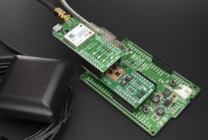
FPGA Test Setup. In the development phase, the NAPA baseband core has been implemented on a Xilinx Virtex6 FPGA device. A Xilinx ML605 development board has been used for the test setup. The main limitation of the testing in this phase was the lack of an analog RF front-end prototype. In order to make early testing of GNSS functionality possible, we adopted a file player developed by Fraunhofer IIS in a previous project. This file player uses a desktop PC to reproduce a digital signal data-stream stored in a binary file on the PC. The stream is sent through a dedicated interface to a commercial digital acquisition board. This board receives a clock synchronized with the baseband core’s clock in the FPGA and delivers the signals directly to the FPGA pins. The complete setup is depicted in Figure 6. The setup in use can be seen on the left part of the opening figure.

Test Board. In the verification phase, which is currently ongoing, the first unpackaged test chip dies have been glued directly to the test PCB and bonded on board without any housing. After receiving the packaged chips, the QFN68 could be regularly soldered on the PCB. A block diagram of the board is depicted in Figure 7. The board hosts the typical switch buttons and LEDs for quick control and status detection as well as some specific interfaces. The clock can be provided through a dedicated SMA clock connector as well as a discrete oscillator. Two sub-miniature push-on (SMP) connectors are also provided for separate the L1 and L5 antenna inputs. The two UART ports, the debugger UART, and the SPI master port are connected using a FTDI chip. This chip allows the simultaneous connection of these ports to a desktop PC’s USB port. A parallel connector is provided to interface external front-end ADC signals and clock. The GPIOs are accessible through the same connector. A dedicated socket is added for a mini-SD card.

Preliminary Results
The chip on the test board was first tested using the same file player of the FPGA setup. This way, we could evaluate the correct functionality of the digital baseband core without the need to activate and configure the on-chip front-end. After the successful tests, we focused on the on-chip front-end configuration, and we used the antenna connectors to provide valid GNSS signals. We tested the chip using three different configurations: a GNSS signal simulator, a static roof antenna, and a small active patch antenna.
In the three configurations, we successfully acquired GPS L1 and Galileo E1 signals. We were also able to perform tracking on GPS L1 and L5I, as well as Galileo E1b and E5aI. Figure 8 shows the spectrum of a snapshot of L1 and L5 paths made using the on-chip dedicated snapshot hardware and sent through the UART port with a dedicated binary protocol for offline processing. For this special test, we used an arbitrary waveform generator to provide noiseless Galileo and GLONASS signals in the L1 and L5 frequency bands, supported by the NAPA chip. After performing a FFT of the two snapshots, we can clearly see these signals. In the L1 plot, the E1b signal is present in the negative frequency range with the two peaks typical of the BOC(1,1) modulation. The FDMA GLONASS G1 is in the positive frequency range with its trapezoidal characteristic. It is also possible to see a side lobe of the E1a BOCcos(15,2.5) in the proximity of the zero frequency. In the L5 plot, we can see the main peak of BPSK E5a signal on the right and its mirrored image on the left, due to the fact that L5 signal path is real.

Acknowledgment
This project has been funded by the Bundesministerium für Bildung und Forschung (BMBF) (German Federal Ministry of Education and Research), which is gratefully acknowledged.


One Comment “Multi-Constellation. Dual-Frequency. Single-Chip.”